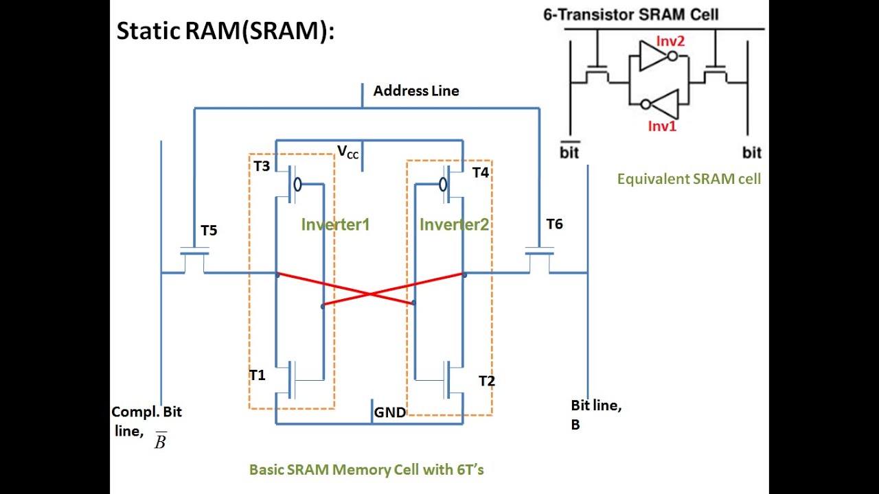
Standard 6t-sram cell circuit 7.3 6t sram cell Past research
7.3 6T SRAM Cell
Sram circuitry Sram writing cell Sram circuit interface memory basic block tutorial diagram asynchronous embedded configuration microcontroller module fundamentals covering systems typical course cypress fig
Sram principle
Schematic for run of the mill sram?Sram floorplan readout circuit structure Embedded systems course- module 15: sram memory interface toSchematic sram mill run circuitlab circuit created using.
Sram bit logic consists structural precharge amplifier outputSram memory dram transistor diagram static block random bit access difference between cell provides complexity density manufacturing resistors advantages dimensions Sram circuit diy bit designing study now diagram followed instructions built veSram interface shifters circuits.
New sram pcb is being built – techtravels.org
Sram cell 6t cmos circuit transistor transistorsSerial sram circuit diagram Sram dram cell vs transistors domain six wikimedia commons credit via figure publicConnecting a 512k*16bit sram (is62wv51216bll-55tli) to a 144-pin stm32.
Sram circuit 6t 5t cellOne-bit sram structural block diagram. it consists of 1-bit 6-t cell Sram 6tSram stm32 512k 16bit connecting fsmc.

Circuit diagram of standard 6t sram figure 2. circuit diagram of
Diagram of the sram cell circuit of the write operation.Sale > sram circuit diagram > in stock Reading and writing operation of sramSram 6t circuit.
Sram-logic block diagramSram consists structural lines precharge reliability Tsmc revealed at iedm 2022 that tsmc's 3 nm hd sram cell is 0.0199 μm²Conventional 6t sram cell..

Sram circuit write
Sram diagram precharge circuit circuits memory stackCircuit sram write buffer complete something should look cl cam hardware teaching ac output Illustration of low-power sram using level shifters as interfaceSram sequential.
Sram 6t conventionalSram principle Study on designing a diy sram circuit, 1 bit for nowSchematic diagram of sram cell.

Sram column with read-write circuitry.
What is the basic idea behind the sram sense amplifier? why do we needSram pcb built being Patents circuit access memory random sramSram memory cell circuit diagrams for (a) standard 6t-sram,.
Dram vs sram1: standard 6t-sram cell circuit The schematic diagram of 8t sram cellComputer laboratory.

Shows the basic 6t sram cell circuit diagram [17]. pu1 and pu2 are the
Sram 8t cell schematicSequential logic High-speed readout sram circuit. (a) global floorplan structure. (bAmplifier sram circuit latch.
Sram lines control data messy wr parallel wires oe circuit loading while only wiring apologize did butSram 6t pu2 Patent us6259623Difference between the sram and dram explained : why dram needed to be.

One-bit sram structural block diagram. it consists of 1-bit 6-t cell
Sram diagram block logic bit which signals data am stack .
.


Schematic for run of the mill SRAM? - Electrical Engineering Stack Exchange

Schematic Diagram of SRAM Cell | Download Scientific Diagram

Connecting a 512K*16bit SRAM (IS62WV51216BLL-55TLI) to a 144-Pin STM32

Past Research - Device and Circuit Lab

7.3 6T SRAM Cell